- 您现在的位置:买卖IC网 > Sheet目录3855 > PIC18LF1230-I/ML (Microchip Technology)IC PIC MCU FLASH 2KX16 28QFN
PIC18F1230/1330
2009 Microchip Technology Inc.
DS39758D-page 113
13.2
Timer1 Oscillator
A crystal oscillator circuit is built-in between pins T1OSI
(input) and T1OSO/TICKI (amplifier output). The place-
ment of these pins depends on the value of Configuration
bit, T1OSCMX (see Section 20.1 “Configuration
). It is enabled by setting control bit T1OSCEN
(T1CON<3>). The oscillator is a low-power oscillator
rated for 32 kHz crystals. It will continue to run during all
power-managed modes. The circuit for a typical LP
oscillator is shown in Figure 13-3. Table 13-1 shows the
capacitor selection for the Timer1 oscillator.
The user must provide a software time delay to ensure
proper start-up of the Timer1 oscillator.
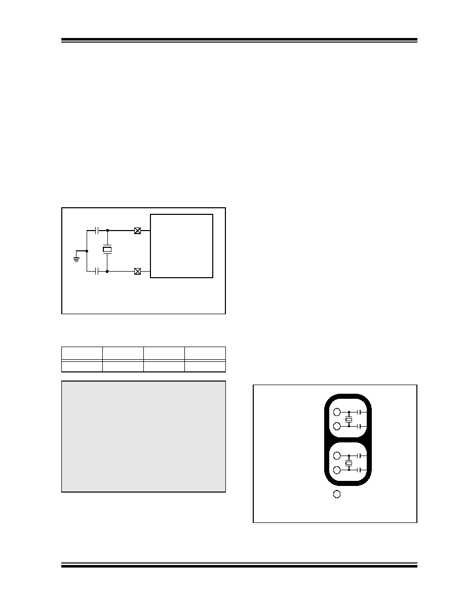
FIGURE 13-3:
EXTERNAL
COMPONENTS FOR THE
TIMER1 LP OSCILLATOR
TABLE 13-1:
CAPACITOR SELECTION FOR
THE TIMER OSCILLATOR
13.2.1
USING TIMER1 AS A CLOCK
SOURCE
The Timer1 oscillator is also available as a clock source
in power-managed modes. By setting the System
Clock Select bits, SCS1:SCS0 (OSCCON<1:0>), to
‘01’, the device switches to SEC_RUN mode; both the
CPU and peripherals are clocked from the Timer1 oscil-
lator. If the IDLEN bit (OSCCON<7>) is cleared and a
SLEEP
instruction is executed, the device enters
SEC_IDLE mode. Additional details are available in
Whenever the Timer1 oscillator is providing the clock
source, the Timer1 system clock status flag, T1RUN
(T1CON<6>), is set. This can be used to determine the
controller’s current clocking mode. It can also indicate
the clock source being currently used by the Fail-Safe
Clock Monitor. If the Clock Monitor is enabled and the
Timer1 oscillator fails while providing the clock, polling
the T1RUN bit will indicate whether the clock is being
provided by the Timer1 oscillator or another source.
13.3
Timer1 Oscillator Layout
Considerations
The oscillator circuit, shown in Figure 13-3, should be
located as close as possible to the microcontroller.
There should be no circuits passing within the oscillator
circuit boundaries other than VSS or VDD.
If a high-speed circuit must be located near the
oscillator (such as the PWM pin, or the primary
oscillator using the OSC2 pin), a grounded guard ring
around the oscillator circuit, as shown in Figure 13-4,
may be helpful when used on a single-sided PCB, or in
addition to a ground plane.
FIGURE 13-4:
OSCILLATOR CIRCUIT
WITH GROUNDED GUARD
RING
Osc Type
Freq
C1
C2
LP
32 kHz
27 pF(1)
Note 1:
Microchip suggests this value as a starting
point in validating the oscillator circuit.
2:
Higher capacitance increases the stability
of the oscillator, but also increases the
start-up time.
3:
Since each resonator/crystal has its own
characteristics, the user should consult
the resonator/crystal manufacturer for
appropriate
values
of
external
components.
4:
Capacitor values are for design guidance
only.
Note:
See the notes with Table 13-1 for addi-
tional information about capacitor selec-
C1
C2
XTAL
PIC18FXXXX
T1OSI
T1OSO/T1CKI
32.768 kHz
33 pF
RB3
RB2
OSC1
OSC2
VDD
Note:
Not drawn to scale.
发布紧急采购,3分钟左右您将得到回复。
相关PDF资料
PIC16LC711-04/SS
IC MCU OTP 1KX14 A/D 20SSOP
PIC18F65K22-I/MRRSL
MCU PIC 32K FLASH MEM XLP 64QFN
PIC16LF87-I/SS
IC MCU FLASH 4KX14 EEPROM 20SSOP
PIC16C62B-20/SS
IC MCU OTP 2KX14 PWM 28SSOP
PIC16LC711-04I/SO
IC MCU OTP 1KX14 A/D 18SOIC
PIC18F66J90-I/PT
IC PIC MCU FLASH 64KB 64-TQFP
ATMEGA32L-8AC
IC AVR MCU 32K LV 8MHZ COM44TQFP
DSPIC30F2012-30I/SP
IC DSPIC MCU/DSP 12K 28DIP
相关代理商/技术参数
PIC18LF1230-I/P
功能描述:8位微控制器 -MCU 4KB 256byt-RAM 16I/O RoHS:否 制造商:Silicon Labs 核心:8051 处理器系列:C8051F39x 数据总线宽度:8 bit 最大时钟频率:50 MHz 程序存储器大小:16 KB 数据 RAM 大小:1 KB 片上 ADC:Yes 工作电源电压:1.8 V to 3.6 V 工作温度范围:- 40 C to + 105 C 封装 / 箱体:QFN-20 安装风格:SMD/SMT
PIC18LF1230-I/SO
功能描述:8位微控制器 -MCU 4KB 256byt-RAM 16I/O RoHS:否 制造商:Silicon Labs 核心:8051 处理器系列:C8051F39x 数据总线宽度:8 bit 最大时钟频率:50 MHz 程序存储器大小:16 KB 数据 RAM 大小:1 KB 片上 ADC:Yes 工作电源电压:1.8 V to 3.6 V 工作温度范围:- 40 C to + 105 C 封装 / 箱体:QFN-20 安装风格:SMD/SMT
PIC18LF1230-I/SS
功能描述:8位微控制器 -MCU 4KBFlash 256byte-RAM 16 I/O 8-bit Family RoHS:否 制造商:Silicon Labs 核心:8051 处理器系列:C8051F39x 数据总线宽度:8 bit 最大时钟频率:50 MHz 程序存储器大小:16 KB 数据 RAM 大小:1 KB 片上 ADC:Yes 工作电源电压:1.8 V to 3.6 V 工作温度范围:- 40 C to + 105 C 封装 / 箱体:QFN-20 安装风格:SMD/SMT
PIC18LF1320-I/ML
功能描述:8位微控制器 -MCU 8KB 256 RAM 16I/O RoHS:否 制造商:Silicon Labs 核心:8051 处理器系列:C8051F39x 数据总线宽度:8 bit 最大时钟频率:50 MHz 程序存储器大小:16 KB 数据 RAM 大小:1 KB 片上 ADC:Yes 工作电源电压:1.8 V to 3.6 V 工作温度范围:- 40 C to + 105 C 封装 / 箱体:QFN-20 安装风格:SMD/SMT
PIC18LF1320-I/P
功能描述:8位微控制器 -MCU 8KB 256 RAM 16I/O RoHS:否 制造商:Silicon Labs 核心:8051 处理器系列:C8051F39x 数据总线宽度:8 bit 最大时钟频率:50 MHz 程序存储器大小:16 KB 数据 RAM 大小:1 KB 片上 ADC:Yes 工作电源电压:1.8 V to 3.6 V 工作温度范围:- 40 C to + 105 C 封装 / 箱体:QFN-20 安装风格:SMD/SMT
PIC18LF1320-I/SO
功能描述:8位微控制器 -MCU 8KB 256 RAM 16I/O RoHS:否 制造商:Silicon Labs 核心:8051 处理器系列:C8051F39x 数据总线宽度:8 bit 最大时钟频率:50 MHz 程序存储器大小:16 KB 数据 RAM 大小:1 KB 片上 ADC:Yes 工作电源电压:1.8 V to 3.6 V 工作温度范围:- 40 C to + 105 C 封装 / 箱体:QFN-20 安装风格:SMD/SMT
PIC18LF1320-I/SOG
功能描述:8位微控制器 -MCU 8kBF 256RM 16I/O Lead Free Package RoHS:否 制造商:Silicon Labs 核心:8051 处理器系列:C8051F39x 数据总线宽度:8 bit 最大时钟频率:50 MHz 程序存储器大小:16 KB 数据 RAM 大小:1 KB 片上 ADC:Yes 工作电源电压:1.8 V to 3.6 V 工作温度范围:- 40 C to + 105 C 封装 / 箱体:QFN-20 安装风格:SMD/SMT
PIC18LF1320-I/SS
功能描述:8位微控制器 -MCU 8KB 256 RAM 16I/O RoHS:否 制造商:Silicon Labs 核心:8051 处理器系列:C8051F39x 数据总线宽度:8 bit 最大时钟频率:50 MHz 程序存储器大小:16 KB 数据 RAM 大小:1 KB 片上 ADC:Yes 工作电源电压:1.8 V to 3.6 V 工作温度范围:- 40 C to + 105 C 封装 / 箱体:QFN-20 安装风格:SMD/SMT